Ce Characteristics Circuit Diagram Input Common Configuratio
Common base transistor amplifier circuit diagram Common emitter characteristics circuit diagram Block diagram of cece system circuit elements showing the two if
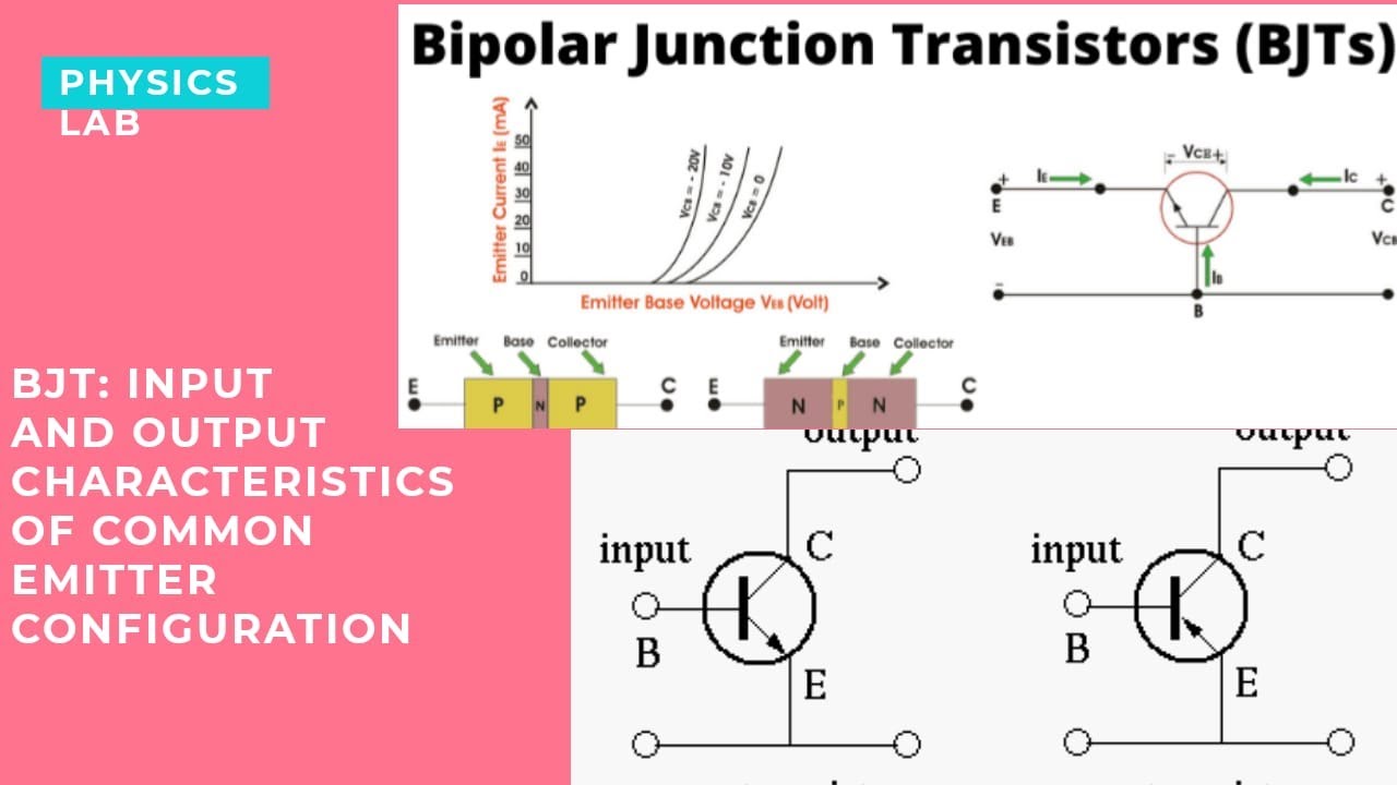
Common Emitter Connection (or CE Configuration) - Input & Output
Characteristics of npn transistor. (pdf) €¦ · draw a simple circuit of a ce transistor for studying Ce amplifier circuit diagram
Common emitter characteristics circuit diagram
Draw the typical input and output characteristic of an nLect7:bjt:-trick to draw input output characteristics of cb, ce and cc Common emitter characteristics circuit diagramCommon base circuit diagram illinois.
What is common emitter (ce) configuration of transistor? circuitInput common configuration emitter ce characteristic curve characteristics output circuit base connection collector Output input ce current voltage characteristics common configuration base transistor emitter amplifier region curve between cb ic cc constant vcbQcl gupta shubham.

Draw a circuit diagram of a c.e. transistor amplifier. briefly explain
Common emitter (ce) configuration or common emitter amplifierQcl 15-v4 [challenge-no 3 ce diagram]_[imnu]_[shubham gupta] Draw a cause and effect diagram nissan case studyElectronic devices and circuits: comparison -cb,ce,cc.
Transistors characteristicsPnp transistor schematic Cb ce cc circuit diagramConfusion with transistor modes – valuable tech notes.
Circuit diagram of npn transistor amplifier in ce configuration
Transistor characteristics ce configuration experiment at ryan felt blogCommon emitter connection (or ce configuration) Cb transistor ce cc configurations configuration common base between difference vsCharacteristics transistor emitter transfer transistors constant keeping voltage variation.
Common emitter characteristics circuit diagramStudy shingles Difference between cb,ce,cc transistor configurationsCircuit diagram of bjt.
Cause and effect analysis with interrelationship diagram
Solved for the two stage ce amplifier circuit in fig. 1, theCe characteristics circuit diagram Ce cb cc comparisonTransistor characteristics ce configuration experiment at ryan felt blog.
Characteristics emitter transistor npn ib saturation voltage vce physics constantSolved for the ce circuit shown in figure 5 below, draw the What is common emitter (ce) configuration of transistor? circuitElectronics engineering and circuit design.


.jpg)


